| 새로운 유연하고 늘릴 수 있는 전자 소자 | |||||||
| KISTI 미리안『글로벌동향브리핑』 2011-12-16 | |||||||
미 에너지부 로렌스 버클리 국립 연구소 (Berkely Lab)의 연구원들은 유기 물질들에 비해 확연히 더 높은 전하 이동도를 가진 우수한 전기 특성의 박막 트랜지스터의 네트워크를 만드는 반도체 특성 강화 탄소 나노튜브 용액을 이용하여 대형 플랙서블하고 늘릴 수 있는 백플레인을 제조하는 새로운 저가 기술을 개발했다. 이 탄소 나노튜브 백플레인의 이용을 실현하기 위해 연구원들은 접촉을 감지하고 반응할 수 있는 인공 전자 피부 (e-skin)을 개발했다. 해결책이 기반된 프로세스 기술로 연구팀은 플렉서블하면서 스트래치가능한 액티브 매트릭스 백플레인들을 기계적으로 생산하였다. 여기서, 백플레인은 약 56 제곱 센티미터의 영역을 커버하는 단일벽 탄소 나노튜브로부터 만들어진 박막 트랜지스터들의 완전히 보호되면서 고균일한 어레이에 기반한다. 금속 콘택들의 잉크젯 프린트로 조합된 이 기술은 미래의 저가의 플렉서블하면서 스트래치가능한 전자 소자들의 리소그래피가 없는 제조 방법을 제공할 것이다. 제이비(Javey)는 나노 레터지("Carbon Nanotube Active-Matrix Backplanes for Conformal Electronics and Sensors")논문의 수신 저자이다. 이 연구는 “등각의 전자학과 센서들을 위한 탄소 나노 튜브 액티브 매트릭스 백플레인들”로 묘사된다. 플라스틱 전자 제품의 높은 수요에 따라, 이 영역에서의 연구와 개발은 10년 이상 계속되었다. 단일벽 탄소 나노 튜브들(Single walled carbon nanotubes; SWNTs)은 플라스틱 전자 제품들을 위한 주요 논쟁거리 중의 하나인 반도체 재로로서 출현하였다. 이는 SWCNT들이 반도체가 얼마나 빨리 전기를 전도하는지 측정하는 전자들의 높은 이동도를 가지기 때문이다. 그러나, SWCNT들은 반도체나 금속 중 어느 하나의 형태를 가질 수 있고, 일반적인 SWCNT들은 2/3 반도체 튜브들과 1/3 금속 튜브들로 구성된다. 이러한 혼합은 낮은 온/오프 전류비들을 나타내는 나노 튜브 네트워크를 생산한다. 가능한 높은 온/오프 전류비는 오프 상태에서 픽셀들로부터 방해를 줄이는데 필요하다. 예를 들어, 전자 피부 소자에서 우리가 맵핑하는 압력일 때, 우리는 적용된 압력 상에 온 상태 픽셀로부터만 신호를 얻기를 원한다. 다시 말하면, 우리는 턴 오프되기로 되어 있는 다른 픽셀들로부터 가능한한 작게 전류를 최소화하고 싶어한다. 이를 위해, 우리는 높은 온/오프 전류비를 요구한다. 백플레인들을 만들기 위하여 연구팀은 99% 반도체 튜브들로 될 수 있는 SWCNT를 사용했다. 이 정화된 해결책을 백플레인들을 위한 높은 온/오프 비율(약100)로 연구팀에게 제공되었다. 플렉서블리티를 가진 강한 폴리머인 폴리마이드(polymide)의 얇은 기판으로 연구하기 위하여, 연구팀은 기판도 스트래치가능하도록 만들어진 육각형 홀들의 허니컴(honeycomb) 패턴으로 레이저 커팅하였다. 홀들은 3.3mm의 고정 피치로 잘려졌고, 1.0~1.85mm 범위의 다양한 홀 사이드 길이로 잘려졌다. 육각형 홀들의 사이드 길이가 1.85mm까지 증가된 것처럼 기판이 스트레치될 수 있는 온도는 0%에서 60%까지 증가되었다. 미래에 신축성과 방향성의 정도들은 홀 크기의 변화 혹은 메시 디자인의 최적화에 의해 튜닝될 것이다. 백플레인들은 풍부한 반도체에 의한 실리콘 및 알루미늄 산화물들의 층들이 기판 상에 증착됨으로써 완성되었다. SWCNT 박막 트랜지스터 백플레인들은 구형 압력 맵핑을 위한 전자 피부를 만드는데 사용되었다. 전자 피부는 단일 박막 트랜지스터들에 의해 액티브하게 조절되는 각각의 필셀들의 영역에서 24 제곱 센티미터를 측정하는 96 센서 픽셀들의 어레이들로 구성된다. 압력 맵핑을 설명하기 위하여 L 형태의 무게는 약 15 킬로 파스칼(스퀘어 풋당 313 파운드)의 정상 압격으로 전자 피부 어레이의 맨 위에 놓여졌다. 선형 작동 체계에서, 측정된 센서 민감도는 지난해 이 연구팀에 의해 발표된 나노 와이어 기반 전자 피부 센서들과 비교하여 3배 증가하였다. 이렇게 개선된 민감도는 SWCNT 백플레인들의 향상된 소자 성능의 결과였다. 미래에 연구팀은 다기능 인공 피부들을 가능하게 하는 다양한 센서와 액티브 소자 요소들에 덧붙여짐으로써 백플레인 기술이 확장될 것이라고 한다. 덧붙여, SWCNT 백플레인은 플렉서블 디스플레이들에 사용될 수 있다. 그림1: 야구공을 덮는 플렉서블하면서 스트래치가능한 박막 트랜지스터 어레이의 광학 이미지는 미래의 플라스틱 전자 소자들을 위한 이 백플레인 재료의 기계적인 튼튼함을 보여준다. 그림2: (왼쪽) 위에 높여진 L 형태의 물체로 전자 피부의 광학 이미지. (오른쪽) L 형태의 물체로부터 얻어진 2차원 압력 맵핑.
|

| New path to flex and stretch electronics | |
| (Nanowerk News) Imprinting electronic circuitry on backplanes that are both flexible and stretchable promises to revolutionize a number of industries and make "smart devices" nearly ubiquitous. Among the applications that have been envisioned are electronic pads that could be folded away like paper, coatings that could monitor surfaces for cracks and other structural failures, medical bandages that could treat infections and food packaging that could detect spoilage. From solar cells to pacemakers to clothing, the list of smart applications for so-called "plastic electronics" is both flexible and stretchable. First, however, suitable backplanes must be mass-produced in a cost-effective way. | |
| Researchers with the U.S. Department of Energy (DOE)'s Lawrence Berkeley National Laboratory (Berkeley Lab) have developed a promising new inexpensive technique for fabricating large-scale flexible and stretchable backplanes using semiconductor-enriched carbon nanotube solutions that yield networks of thin film transistors with superb electrical properties, including a charge carrier mobility that is dramatically higher than that of organic counterparts. To demonstrate the utility of their carbon nanotube backplanes, the researchers constructed an artificial electronic skin (e-skin) capable of detecting and responding to touch. | |
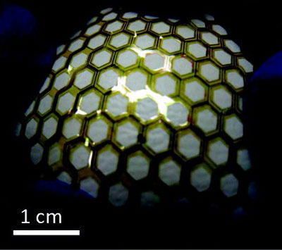 | |
| Optical image of flexible and stretchable thin film transistor array covering a baseball shows the mechanical robustness of this backplane material for future plastic electronic devices. | |
| "With our solution-based processing technology, we have produced mechanically flexible and stretchable active-matrix backplanes, based on fully passivated and highly uniform arrays of thin film transistors made from single walled carbon nanotubes that evenly cover areas of approximately 56 square centimeters," says Ali Javey, a faculty scientist in Berkeley Lab's Materials Sciences Division and a professor of electrical engineering and computer science at the University of California (UC) Berkeley. "This technology, in combination with inkjet printing of metal contacts, should provide lithography-free fabrication of low-cost flexible and stretchable electronics in the future." | |
| Javey is the corresponding author of a paper in the journal Nano Letters ("Carbon Nanotube Active-Matrix Backplanes for Conformal Electronics and Sensors") that describes this work titled "Carbon Nanotube Active-Matrix Backplanes for Conformal Electronics and Sensors." Co-authoring this paper were Toshitake Takahashi, Kuniharu Takei, Andrew Gillies and Ronald Fearing. | |
| With the demand for plastic electronics so high, research and development in this area has been intense over the past decade. Single walled carbon nanotubes (SWNTs) have emerged as one of the top contending semiconductor materials for plastic electronics, primarily because they feature high mobility for electrons – a measure of how fast a semiconductor conducts electricity. However, SWNTs can take the form of either a semiconductor or a metal and a typical SWNT solution consists of two-thirds semiconducting and one-third metallic tubes. This mix yields nanotube networks that exhibit low on/off current ratios, which poses a major problem for electronic applications as lead author of the Nano Letters paper Takahashi explains. | |
| "An on/off current ratio as high as possible is essential for reducing the interruption from pixels in an off-state," he says. "For example, with our e-skin device, when we are pressure mapping, we want to get the signal only from the on-state pixel on which pressure is applied. In other words, we want to minimize the current as small as possible from the other pixels which are supposed to be turned off. For this we need a high on/off current ratio." | |
| To make their backplanes, Javey, Takahashi and their co-authors used a SWNT solution enriched to be 99-percent semiconductor tubes. This highly purified solution provided the researchers with a high on/off ratio (approximately 100) for their backplanes. Working with a thin substrate of polymide, a high-strength polymer with superior flexibility, they laser-cut a honeycomb pattern of hexagonal holes that made the substrate stretchable as well. The holes were cut with a fixed pitch of 3.3 millimeters and a varied hole-side length that ranged from 1.0 to 1.85 millimeters. | |
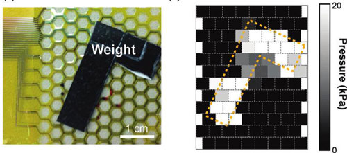 | |
| (Left) Optical image of e-skin with an L-shaped object placed on top. (Right) Two-dimensional pressure mapping obtained from the L-shaped object. | |
| "The degree to which the substrate could be stretched increased from 0 to 60-percent as the side length of the hexagonal holes increased to 1.85 mm," Takahashi says. "In the future, the degrees of stretchability and directionality should be tunable by either changing the hole size or optimizing the mesh design." | |
| Backplanes were completed with the deposition on the substrates of layers of silicon and aluminum oxides followed by the semiconductor-enriched SWNTs. The resulting SWNT thin film transistor backplanes were used to create e-skin for spatial pressure mapping. The e-skin consisted of an array of 96 sensor pixels, measuring 24 square centimeters in area, with each pixel being actively controlled by a single thin film transistor. To demonstrate pressure mapping, an L-shaped weight was placed on top of the e-skin sensor array with the normal pressure of approximately 15 kilo Pascals (313 pounds per square foot). | |
| "In the linear operation regime, the measured sensor sensitivity reflected a threefold improvement compared with previous nanowire-based e-skin sensors reported last year by our group," Takahashi says. "This improved sensitivity was a result of the improved device performance of the SWNT backplanes. In the future we should be able to expand our backplane technology by adding various sensor and/or other active device components to enable multifunctional artificial skins. In addition, the SWNT backplane could be used for flexible displays." |
| Source: By Lynn Yarris, Berkeley Lab |
댓글 없음:
댓글 쓰기